Front Panel Logic Card construction [completed 1/26/2004]
The front panel consists of a wire-wrap card to hold the logic, and
(connected by a pair of 50-line ribbon cables) an assembly holding the switches
and LEDs. This will be the first card to build. For one thing, it is
the easiest and least-dense card - good for me to hone my wire-wrapping and
layout skills. Secondly, it contains the clock circuitry which is required
by all of the other card.
Initially, I'll build a throw-away switch/LED assembly to be used for
testing. With that, I should be able to fully test the clock generation, as
well as the reset and power-on circuitry.
1/26/2004
Testing went much faster than I thought it would. Once I had things set
up, I was able to invidually test the latching of each bit for the IR and L bus
displays. I first attached a pull-down resistor to the latch clock, and
then clipped in my logic pulser. For each bit, the led drive output
was clipped to my test LED on the front panel, and I pulsed in a 0, 1 and then 0
from the backplane D bus and L bus inputs. All clear - no errors.
The board is now fully tested (as far as I can). Ship it...
1/25/2004
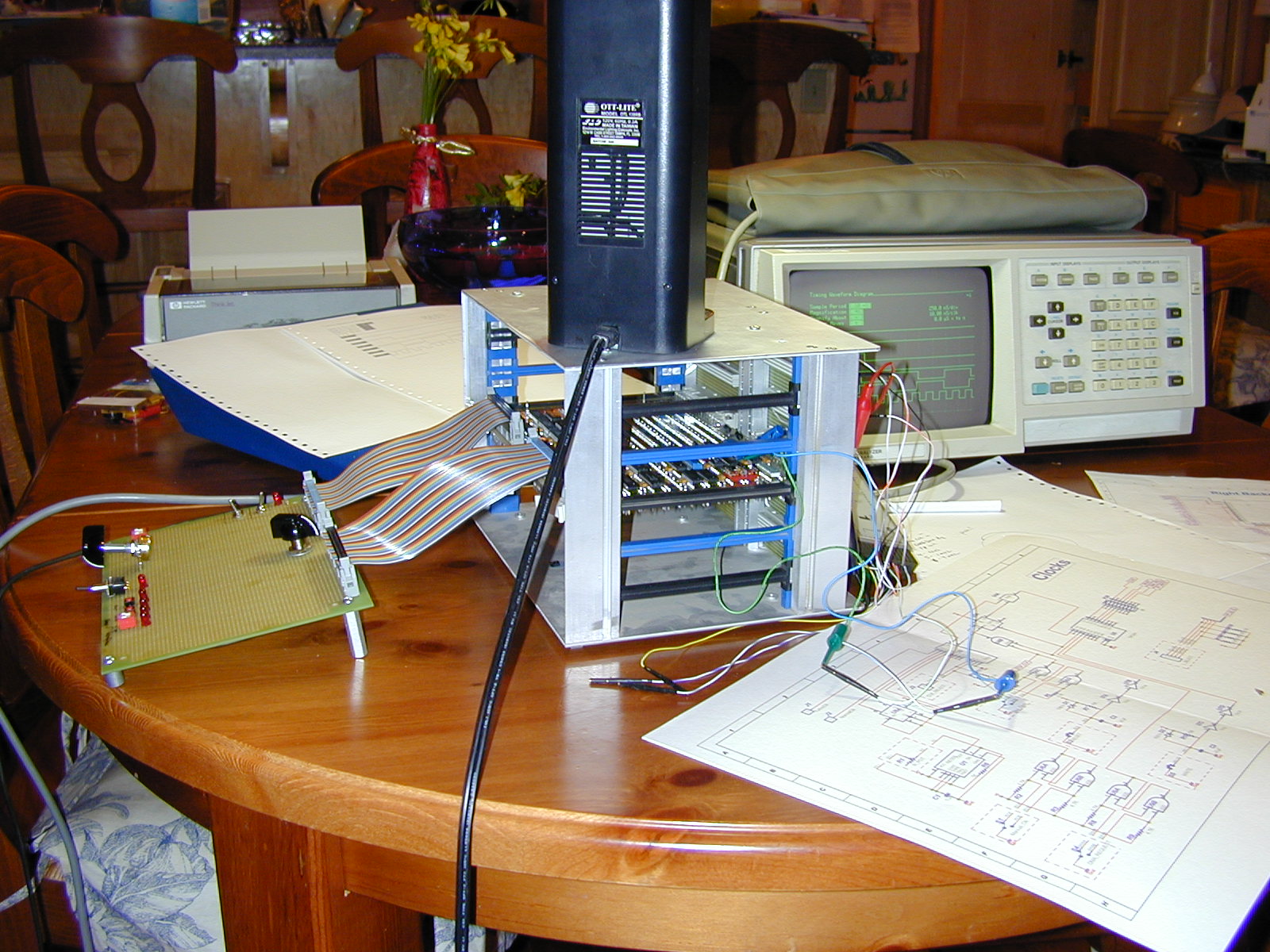
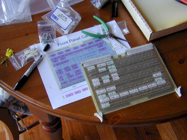
Weekend ended up busier than I expected - only got to spend an hour or so
testing the fp logic card. I still don't have a dedicated area in
the house, so had to commandeer the kitchen table (and then clear it off before
dinner):
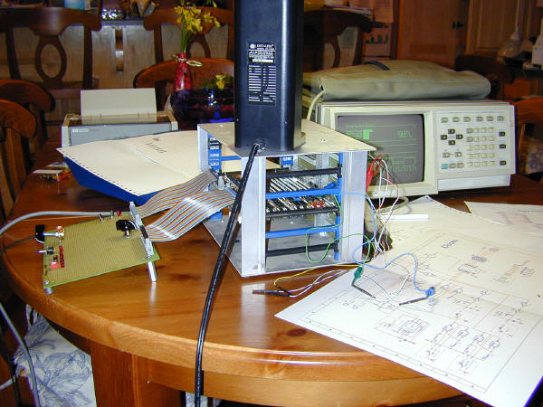
Had enough time to validate (again) the proper behavior of _RESET and
_STOP_CLK. Ran into a minor problem with _DMA_REQ and _FP_WRITE.
They appear to be reversed on the backplane. They behaved properly, but
seem flipped. Didn't have time to look into it - it's possible I just set
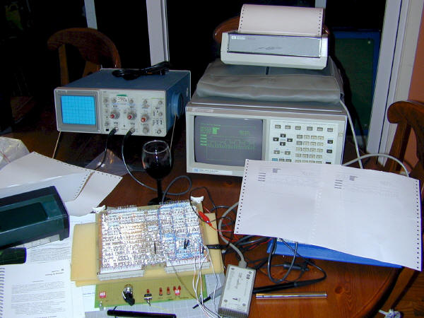
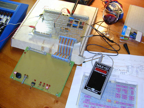
up the logic analyzer wrong. This was my first testing with the card in
the cage using the old backplane, so I wanted to see what the clock looked like
on the back plane. Here's a picture using my 60 MHZ tek scope:
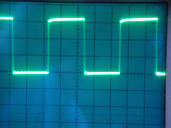
Of course, I'm just a software guy, but this looks to me to be a pretty clean
signal. I'm using the termination scheme suggested by David C. - running
the clocked signals through a resister before they hit the bus. I'm using
62 ohms now, but I'll play with that value once I get everything loaded.
I'm guessing I'll need 3 or 4 hours to fully test the fp logic card (assuming
no failures). Unfortunately, it may take a week of calendar time for me to
find that 3 or 4 hours of uninterrupted quiet.
[update - after the kids went to bed, the house was quiet so I got a lot of
the testing out of the way. All of the LED drive stuff worked fine, and
I've verified correct wiring on _DMA_REQ and _FP_WRITE. Must have mixed
those two up during logic analyzer setup. Still have the hard testing -
the latches for IR and L. Not sure yet how I'm going to test those.
Most likely set up the inputs with test clips to power and ground to give me an
interesting bit pattern. Then, use the logic pulser to send in the latch
signal. I've sort-of already tested the L bits. The latch for these
is the transparent 74F533. I don't have the clock signal connected there,
but as TTL tends to show unconnected inputs as logic high, it just happened that
the inputs passed through to the outputs (and tested as expected). Still,
want to do a proper test of these.]
1/23/2004
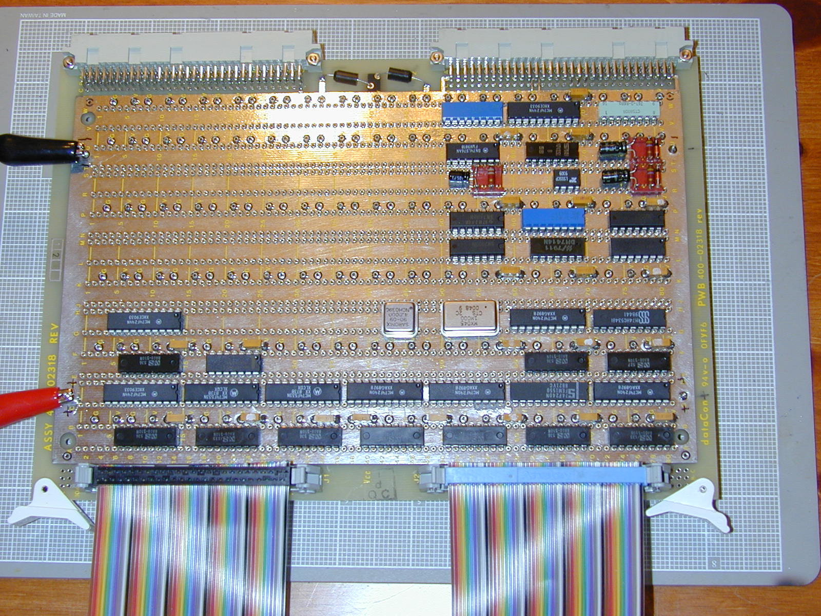
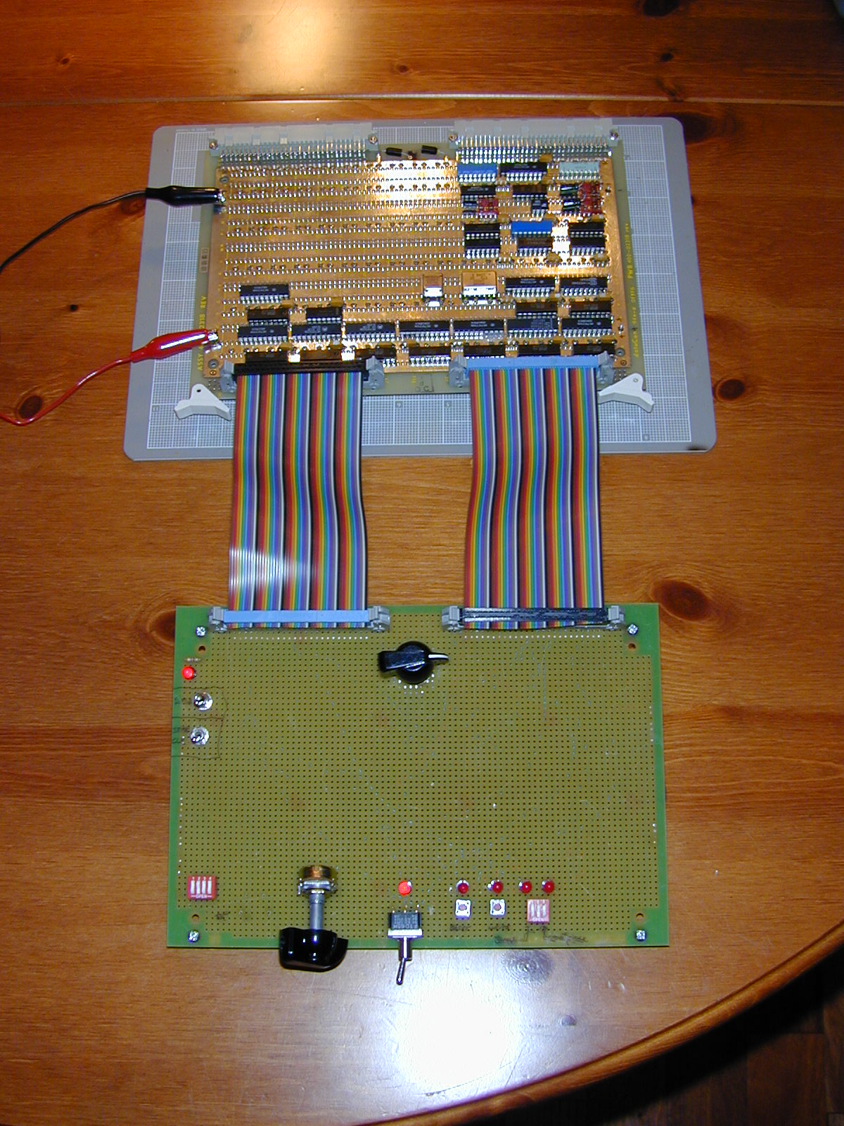
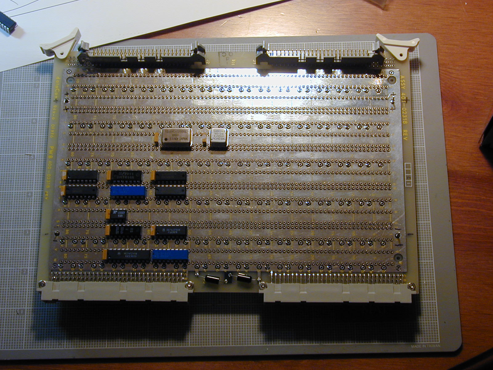
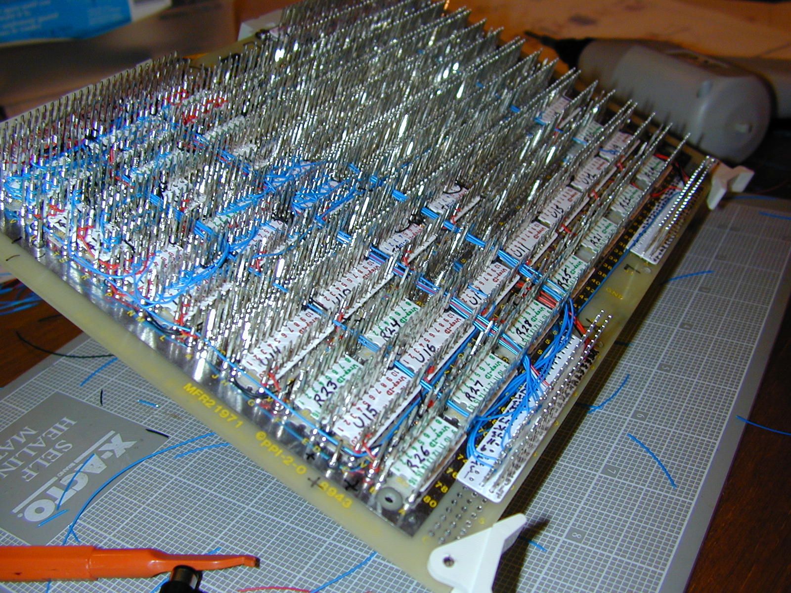
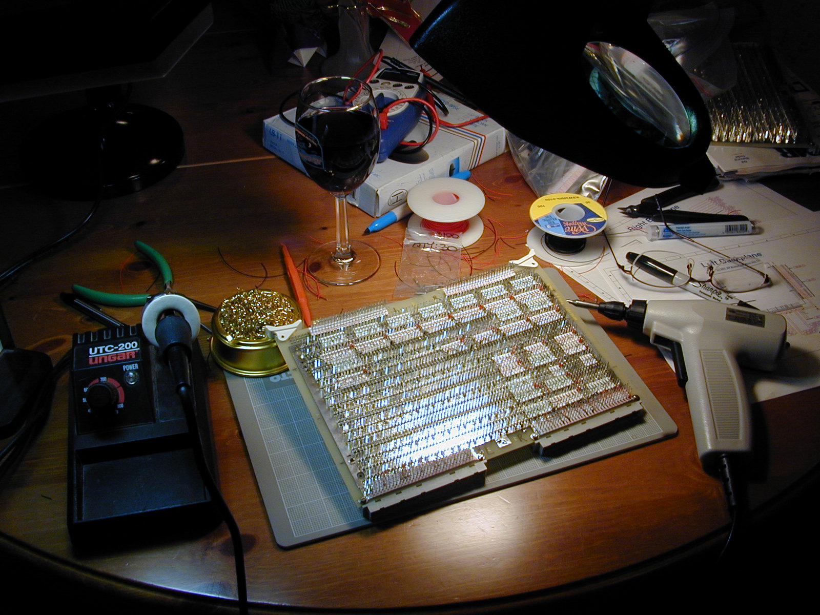
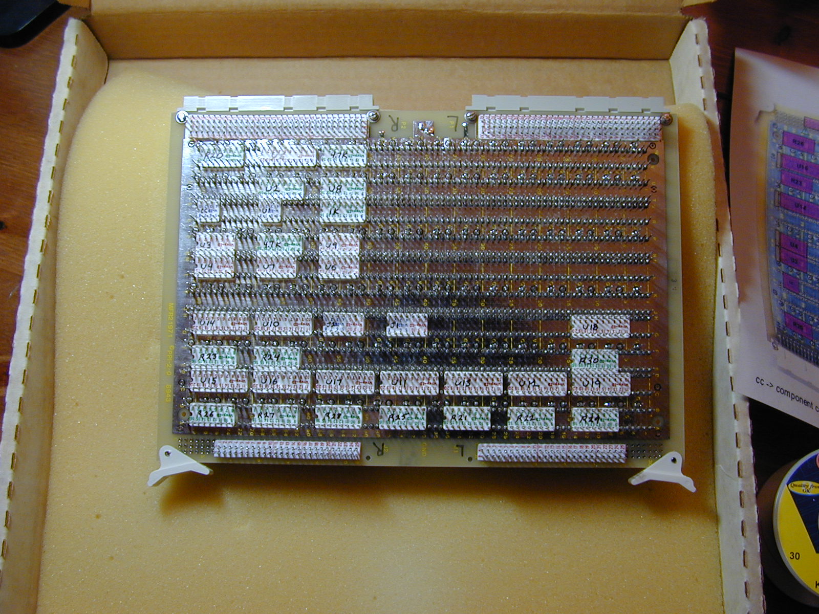
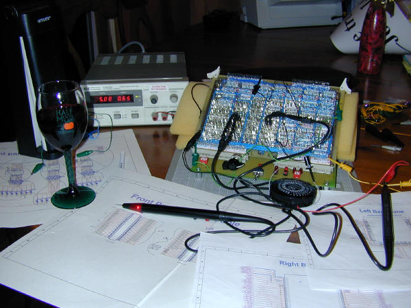
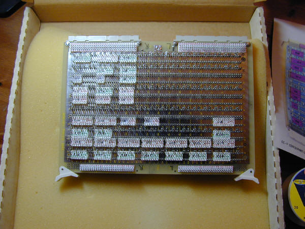
Completed construction of the front panel logic card, but not without a bit
of a mess. First, though, here are some photos:

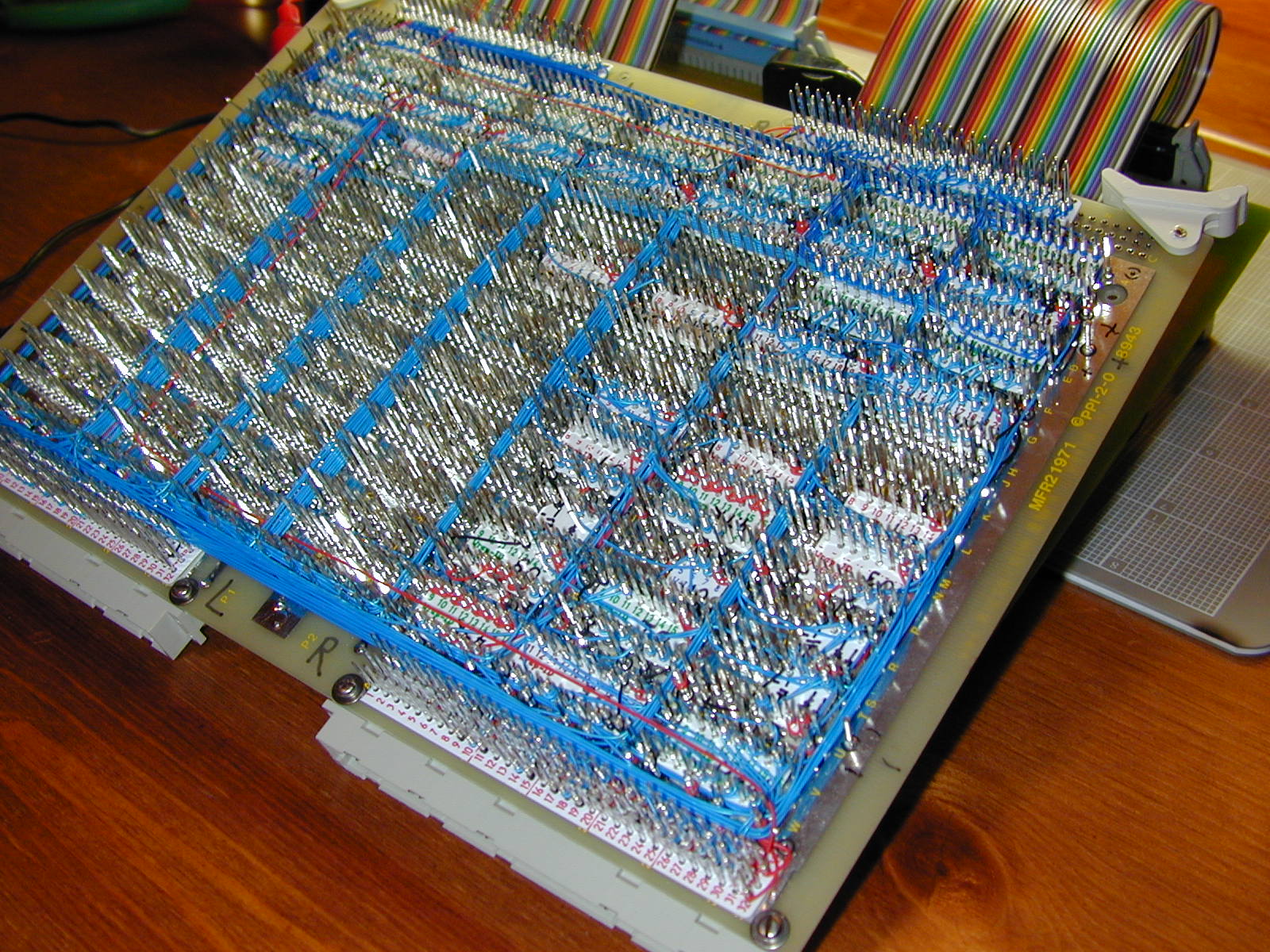
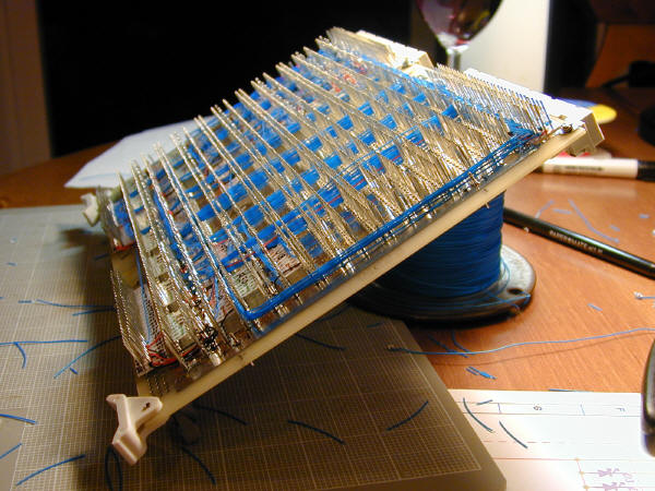
... and the wire wrap side:

...and connected to the temporary front panel switch assembly:
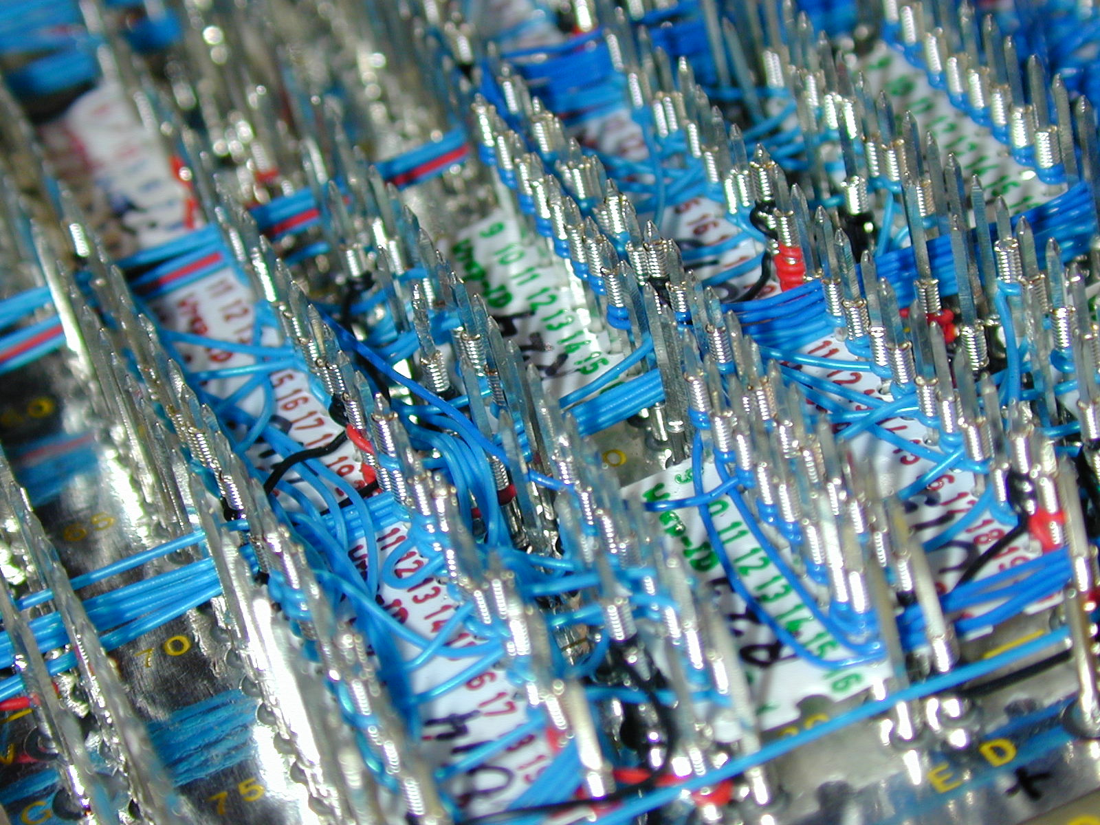
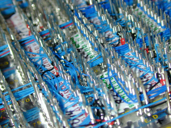
...and now, how about a close-up of that wild wire wrap:
Okay, now a bit about the final steps. I only had a few wires to run,
and they went in very smoothly and quickly. I don't want to say it
out loud, but I think I'm seeing a definite improvement in my wire wrapping
technique. Very few snapped wires this time. Anyway, after all of
the wires were in, the next step was to solder in the bypass capacitors.
This proved a bit tricky. The socket holes for power/ground on the
component side of my boards are large - too large to just press fit my caps.
It was difficult to solder the leads in, though, because the sockets were
connected to the ground and vcc planes - which proved to act as heat sinks.
It was tough to avoid cold solder joints. But, with a bit of patience
things were moving along.
At least there were until I noticed the spill. Somehow I had dropped a
large glob of solder onto the board. It spattered across a 4-hole space,
shorting those pins to Vcc and filling one of the socket holes. What a
mess! First I tried to use the tip of my soldering iron to scrape the
solder away. It just spread it around and made it worse. Next, I
tried one of those spring-loaded solder sucker things. No go. My
biggest problem was that the Vcc plane was acting as a heat sink. If it
got the solder hot enough to melt, so was the general region of the board - and
the solder just flowed deeper.
I thought about just abandoning that region of the board, but as luck would
have it that particular chip area was home to one of the more difficult to route
and densely packed wire area. Re-doing it would have been a mess.
Finally, though, I decided to go with a strategy that worked out well. I
got out my Dremel tool, and using a very small drill bit I drilled out the
solder (and Vcc plane) around each of the shorted pins. I then used my
smallest drill bit, spinning it with my fingers, to clear the one socket hole
that had been closed up by the solder spill. Dodged tragedy again there: I
had cleared to hole pretty good, and decided to do one last little cleanup pass
with my tiny drill bit. Should have left well-enough alone - snapped the
damn drill bit off in the socket. Luckily a tiny bit of it stuck out, and
after about a dozen tries with my needle-nose pliers was able to pull it out.
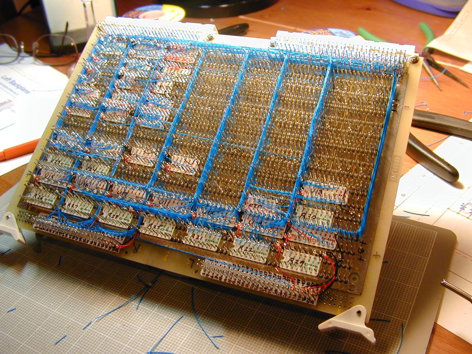
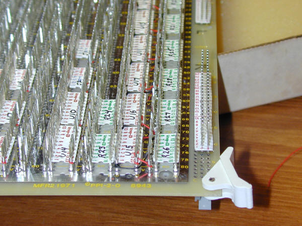
Anyway, here's the repaired area:
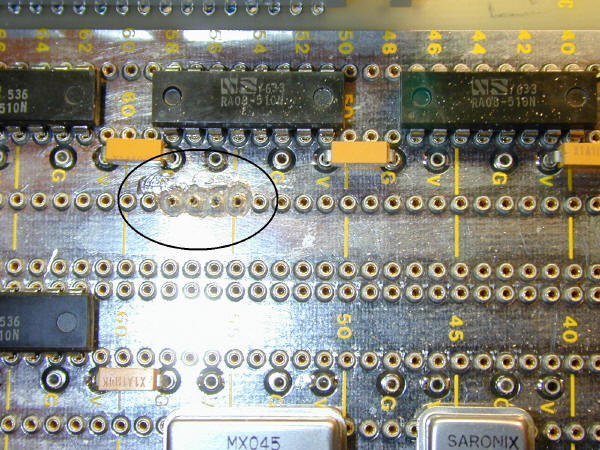
Ugly, but it all worked out.
Haven't done comprehensive testing on the board yet. This is likely to
take a while - with all of the LED drivers, this board generates a lot of
signals.
1/19/2004
Getting pretty close to finishing the wire wrapping, but as the board becomes
denser with wires the slower it's going. I'm getting a lot more bad wraps
and snapped wires that have to be redone - a result, I think, of all of the
routing and tight squeezes. I think the floor plan I'm going to use on
subsequent cards will help. Also, this card has a lot of signals that
cross the board (bus signals going to the LED drive circuitry and then on to the
ribbon cables. I think that makes things worse (lots of long lines), but
then again this is the least densely populated board. Building this
machine is going to be tricky.

All but a couple of the signals needed from the bus (top edge of above photo)
are now in, so my main traffic problem is over. What's left is wiring up
the LED drivers and the ribbon cable (mostly bottom two rows of the card).
Should be able to finish in a couple of evenings work.
1/18/2004
Finally got to really use my logic analyzer and oscilloscope. I picked
these up on eBay (where else...) really cheap over the last couple of years, and
have been waiting until I had a chance to use them. Not only do they work,
but they helped me discover some minor problems with my reset circuitry. I
have a flip-flop to gate my system clock (CLK_S) and clamp it low if there's a
reset or the StopClock toggle switch is thrown. For StopClock (a debugging
switch which allows me to safely change clock sources), it all worked great - it
waits until a falling edge and then clamps low. However, for _RESET I
don't want to wait for the next naturally occurring falling edge - I want to
force things low immediately. The logic analyzer made my mistake clear
quickly, and it only took a minor change (clear the flip-flop on _RESET) to fix
it all.
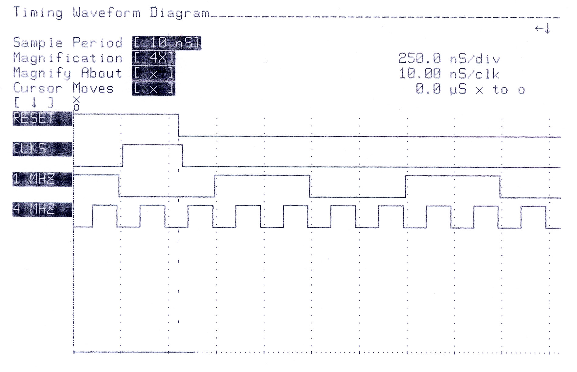
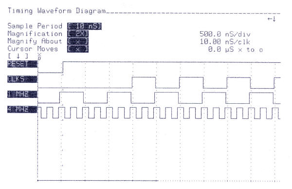
Here's a waveform view of the reset button getting pushed. In this
case, the 1MHZ clock is selected (the selected clock source is inverted yielding
CLK_S). Note that it now goes low on _RESET,
rather than waiting for the next normal falling edge (as _STOP_CLK behaves).

And, here's what things look like when reset deasserts. Note that we
pause a bit before starting up CLK_S (by design).
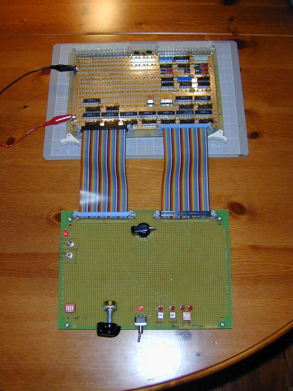
Next up is finishing the wiring on the front panel logic card - which largely
involves driving a bunch of LEDs. With luck, I should be able to finish
off the entire card within a couple of days.
1/17/2004
Got my first signs of life tonight. I spent a couple of hours building
up the throw-away front panel assembly (switches & LEDs) - it only has a small
subset of the things the real front panel will hold, and I expect I'll add more
to it as time goes on. Anyway, I hooked it all up and started tracing
clock signals. Three of my four clocks worked great - the single-step
clock (toggle switch on front panel assembly), 555-timer based variable clock
(pot on fp assembly) and my high-speed oscillator. The low-speed
oscillator didn't immediately show up at the mux, but I may have just plugged it
in wrong. Will debug that later. Anyway, it's nice to see signals
showing up. I'll be testing the reset circuitry, stop clock, the
clock mux and the dma request line.
1/12/2004

Boy, do I feel stupid. No, wait. Actually I really am stupid.
A long time ago I tried to determine the best layout for my wire wrap cards.
My most common chips are in 20 pin packages. Because I wanted to add a
decoupling capacitor to each chip and I had a supply of 2-pin dip 0.1uF caps, I
figured I'd just allocate 22-pin spaces across the board (two rows of 11 holes).
I knew it would be tight when putting back-to-back 20-pin packages, but I
grabbed a couple of chips from my parts bin and found that it would all fit.
Unfortunately, I was not bright enough to consider that some packages are bigger
than others. Most of which hang over the edge enough that there is no room
for my decoupling capacitors. I did not realize this until tonight.
I had completed all of the wire wrap needed for clock generation, and I decided
to go ahead and populate the board for testing. Some parts simply will not
fit with the decoupling capacitors in place.
I could mount the caps elsewhere, but you want to get them close to Vcc.
At the moment, I think my plan is to just consider all of the work on this board
to be wire-wrap practice. I'll go ahead and do some logic testing of the
clock circuits - they should still work just fine. But after that's done,
I'll rip out all of the wires, redo the layout, and start over. I do
have some spare boards - so I might just start fresh with one of them.
Ouch.
[Update after sleeping on it: I won't be tossing the board. Things will
work out just fine if I solder the caps into the power and ground pin sockets
that run in the channels along side the chip channels. I would have used
those pin sockets from the start, but for some reason they are much larger holes
than the regular sockets. Should work fine with solder, though. Or,
if that doesn't work, I can just shave down the plastic packages of the chips
that hang over the edge (thanks Ron!).
1/11/2004

Making good progress - am only 40 or so wraps from completing the clock
generation portion of the card. Once that's done, I'll do my first
power-on testing. Having a bit of a frustrating time with the wrapping,
though. When using the blue AD-Wrap, I need to have just a tiny amount
more of up pressure on the wrap than I do with the OK red and black wire - and I
end up snapping off about 20% of the time. I've ordered the Standard
Pneumatic bit/sleeve set, and it should arrive by the end of the week. I'm
hoping that will help.
1/9/2004

Solved my wire wrapping problems. The old bit and the OK gun using OK
wire works just fine. And, the slack issue is taken care of by holding
down the wire prior to the second wrap with the little orange hand tool in the
picture above. All of the power and ground wiring on the board is now
complete (oh, except for the ribbon cable header - putting that off until last).
Really getting my wire-wrap rhythm going now after that early scare. The
last 100 or so wraps went without error. I only needed to remove and redo
one wire, because it didn't have quite the amount of slack I was shooting for.
Next up is to apply power to the board and test it out. Perhaps tomorrow.
After that, I'll start doing the logic wiring - beginning with the oscillators
and working outwards. Perhaps I'll have actual signals to look at on the
oscilloscope soon!
1/7/2004
Finished placing the IDs and soldered in the two 50-pin ribbon cable sockets,
as well as a couple of 10uF tantalum caps where power enters the board.
Ran into problem when I started to wire-wrap. I plan on using
cut-strip-wrap, but I couldn't get my new expensive bit to work. It's
still possible that it's my technique, but I don't think so. The bit
doesn't fit well in the sleeve, and the wire doesn't slide cleanly into the
channel. I was finally able to proceed by using the old cut-strip-wrap bit
that Gil Smith gave me. In 40 or so wraps, I had only one wire snap - and
it was clearly my fault (too much pressure on the gun). The bit is old and
worn, though, and I do have a problem with the stripped insulation getting
jammed in the channel, forcing me to remove the bit from the sleeve. That
happed six or seven times. I think I'm going to check into the bit/sleeve
set by Standard Pneumatic.
I'm sure I still have a ways to go before my technique is really good. I
think I'm most of the way there (and I have done a few thousand wraps with this
gun and pre-stripped wire with a regular bit). My biggest issue is that if
I don't hold onto the loose end of the wire, it will spin it around the post
(the insulated portion) before cutting & stripping. It's pretty easy to
get it right when putting on the first end of a wire, but I'm not doing to well
on the other end. What seems to happen is that the wire will get pulled
taught. This, I think, is bad. If I get a taught wire across the
corner of another pin, it could cut through the insulation and short.
However, if I leave enough slack for me to hold on with my fingers, I'll end up
with too much slack.
Guess I just need to keep practicing - and perhaps I should make a stick-like
tool to hold onto the wire before making the 2nd wrap.
Anyway, I am starting with the power/ground wiring, including the bypass
capacitors. About 20% complete, and it looks like this:
1/4/2004
First step - add the wire-wrap IDs. Didn't have quite enough on hand,
so will have to make a run to Anchor Electronics tomorrow. Want to be
especially careful getting these things right. I notice that the row
numbering on the 96-pin connectors is flipped relative to my IDs. On the
board, the mask says C B A, while my IDs run A B C. I had an issue with
this when doing the backplane. Doesn't really matter, so long as I'm
consistent.
Also, will need to make my own IDs for the 50-pin wire-wrap connectors.
I think the easiest thing to do will be to cut down some 96-pin ids.